Leipziger nanoAnalytikum (LenA)
Wissenschaftliche Plattform für Materialanalyse auf atomarer Ebene
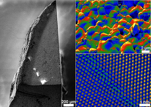
Eine wichtige Voraussetzung für die Entwicklung innovativer Materialien und Oberflächen mit gewünschten Eigenschaften ist die Erforschung ihrer atomaren Struktur und chemischen Zusammensetzung. Daher ist die nanoskalige Analyse in der Materialforschung von außerordentlicher Bedeutung. Am IOM wird diese am Leipziger nanoAnalytikum (LenA) durchgeführt. In dessen Zentrum steht ein analytisches aberrationskorrigiertes Transmissionselektronenmikroskop (TEM). Da die Dicke einer TEM-Probe weniger als hundert Nanometer betragen sollte, bietet das LenA Zugang zu verschiedenen TEM-Präparationsmethoden. Die Forschungsaktivitäten am LenA liegen im Bereich der Aufklärung der realen Struktur von nanoskalige Materialien sowie der Untersuchung dynamischer Prozesse mittels in-situ TEM. Aufgrund der Multidisziplinarität der Forschung ist das Leipziger nanoAnalytikum zudem Partner in nationalen und internationalen Forschungsprojekten.
Expertise
- Aberrationskorrigierte hochauflösende Rastertransmissionselektronenmikroskopie
- In-situ Transmissionselektronenmikroskopie
- Strukturaufklärung von Nanostrukturen, Grenzflächen und Defekten
- Dünne Schichten und Heterostrukturen
Highlights
Van der Waals interfacial bonding and intermixing in GeTe-Sb2Te3-based superlattices
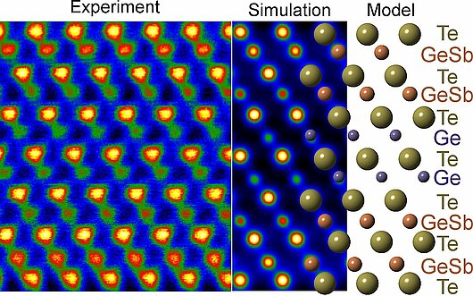
A. Lotnyk, I. Hilmi, U. Ross, B. Rauschenbach
Nano Research 11(2018) 1676-1686
https://doi.org/10.1007/s12274-017-1785-yAdvanced scanning transmission electron microscopy analysis in combination with image simulation reveal the local structure and interlayer bonding within of GeTe-Sb2Te3-based heterostructures prepared by pulsed laser beam assisted deposition. The knowledge can be used for the development of chalcogenide-based heterostructures with well-defined microstructure.
In situ observations of the reversible vacancy ordering process in van der Waals-bonded Ge-Sb-Te thin films and GeTe-Sb2Te3 superlattices
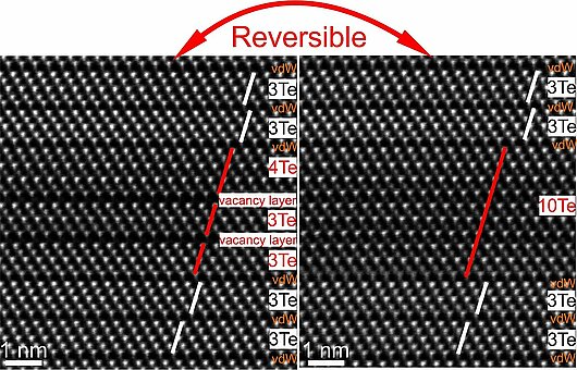
A. Lotnyk, T. Dankwort, I. Hilmi, L. Kienle, B. Rauschenbach
Nanoscale 11 (2019) 10838-10845
https://doi.org/10.1039/C9NR02112DThis work reports on nanoscale observations of structural rearrangements in van der Waals bonded GeTe-Sb2Te3-based thin films and superlattices using in situ experiments inside an aberration-corrected transmission electron microscope. Experimental findings reveal a reversible self-assembled reconfiguration of the structural order in the studied materials, which is associated with the ordering of structural vacancies into ordered vacancy layers and with readjustment of lattice plane distances within newly formed structures, the processes and structural configurations that have never been observed before in such compounds.
“Stickier”-Surface Sb₂Te₃ Templates Enable Fast Memory Switching of Phase Change Material GeSb₂Te₄ with Growth-Dominated Crystallization
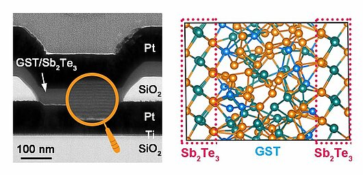
J. Feng, A. Lotnyk, H. Bryja, X. Wang, M. Xu, Q. Lin, X. Cheng, M. Xu, H. Tong, X. Miao
ACS Applied Materials & Interfaces 12 (2020) 33397-33407
Link
This work shows that GeSb2Te4-Sb2Te3 heterostructures prepared by pulsed laser beam assisted deposition can improve writing times of memory devices. Microstructural study of memory cells in combination with ab initio molecular dynamical simulations reveal that the improvement in device performance is due to the enhancement in crystallization rate of amorphous GeSb2Te4 from crystalline Sb2Te3 surface, which possesses a sticky properties to attract Ge interfacial atoms more effectively than intrinsic GeSb2Te4 surface.Exploding and weeping ceramics
H. Gu, J. Rohmer, J. Jetter, A. Lotnyk, L. Kienle, E. Quandt, R.D. James
Nature 599 (2021) 416-420
https://doi.org/10.1038/s41586-021-03975-5Ceramics are materials being used in the daily life of humans since their discovery. The applications of ceramics are ranging from electronic to medical devices. However, the ceramics are brittle and the materials shatter by the slightest deformation. An international research team from the Kiel University (CAU, Germany), the Leibniz Institute of Surface Engineering (IOM, Germany) and the University of Minnesota (UMN, USA) have discovered a new route to synthesize a reversible shape memory ceramic, offering new applications for the materials. Advanced transmission electron microscopy proves a chemically homogeneous ceramic system at the nanoscale and the absence of short-range ordering, where both impact the properties and functionality of such materials.
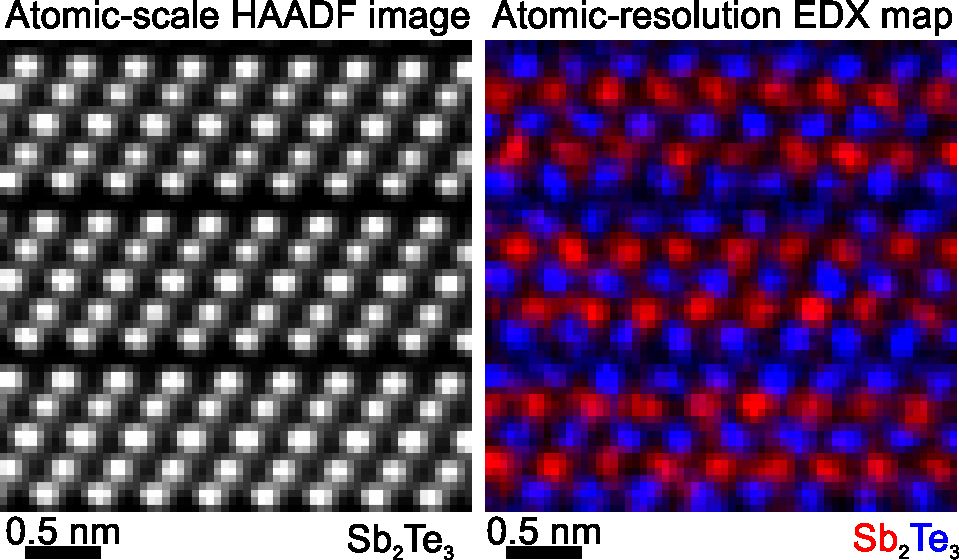
Epitaxial layered Sb2Te3 thin films for memory and neuromorphic applications
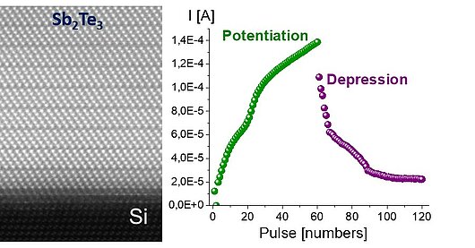
H. Bryja, J.W Gerlach, A. Prager, M. Ehrhardt, B. Rauschenbach, A. Lotnyk
2D Materials 8 (2021) 045027
https://doi.org/10.1088/2053-1583/ac1e71
2D materials have attracted a lot of attention as active layers in memristive devices owing to their high downscaling potential and easy stacking due to van der Waals forces. This work introduces epitaxial 2D-like Sb2Te3 thin films as a novel active layer for memristive devices with analog programmability. The response of such memory cells can be used to mimic synaptic behaviours of biological systems, thus showing a high potential of single-crystalline Sb2Te3 thin films for neuromorphic applications. The Sb2Te3 thin films were directly grown on microelectronics-relevant Si substrates by pulsed laser deposition using low deposition temperatures. This offers an industry applicable large-scale method for device fabrication in addition, circumventing major challenges in the integration of 2D materials.