The ever-increasing demand for high-precision structured surfaces for optical and microelectronic applications requires not only the improvement of existing manufacturing technologies, but also the development of new approaches that can contribute to the realisation of more sustainable manufacturing technologies. The use of atmospheric plasmas is one approach to reducing energy consumption in micrometer structuring.
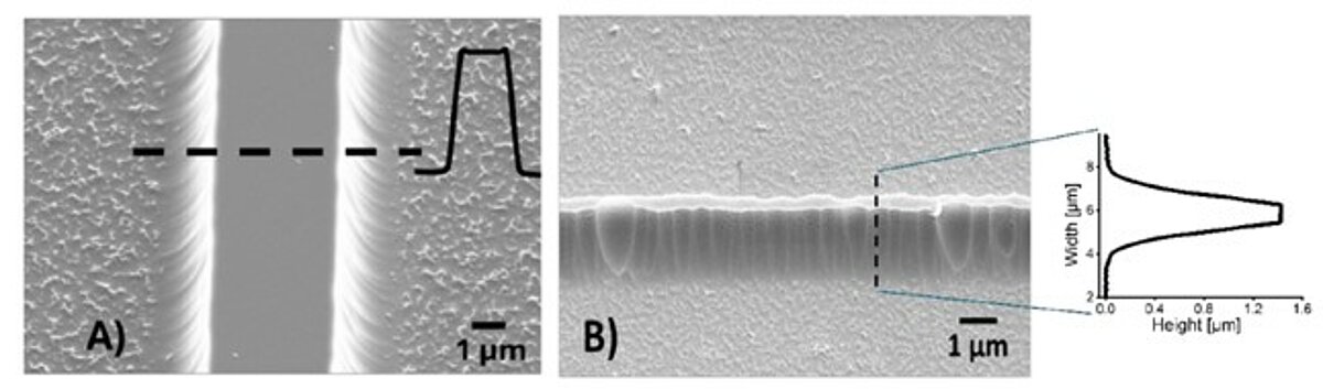
Researchers in the ‘Ultra-precision Surfaces’ field of research at the Leibniz Institute of Surface Engineering (IOM) have now succeeded in developing a cost-effective method for transferring micro-patterns into quartz glass that does not require expensive vacuum systems. With the help of reactive plasma jets applied at atmospheric pressure, line patterns with a width of 2.5 to 50 micrometres can be successfully transferred into quartz glass. This dry etching process bypasses conventional wet etching processes involving aggressive chemicals and represents an environmentally friendly and more efficient alternative for microstructuring. Compared to conventional vacuum processes, which require expensive and complex equipment and are limited by high costs and a restriction on component size, this method enables more flexible and scalable manufacturing. Furthermore, the high plasma etch rates of about 200 nanometers per second allow faster structuring compared to conventional methods.
The method offers great potential for applications in micromechanics and optics, particularly for the production of micro-opto-electro-mechanical systems (MOEMS).
The results of the study were published in the journal Applied Surface Science Advances under the title: Transfer of micron pattern with reactive atmospheric plasma jets into fused silica.
Further information is available at: https://doi.org/10.1016/j.apsadv.2024.100636