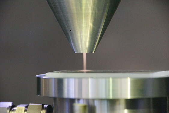
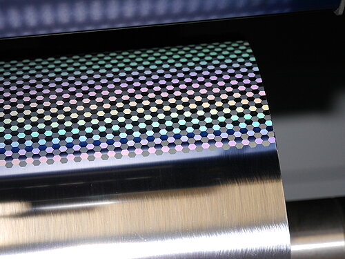
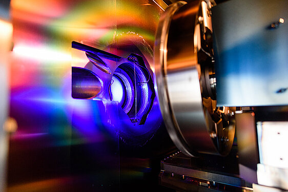
The field of research investigates beam-based technologies for ultra-precise processing of surfaces, near-surface areas and thin films. The work focuses on application fields in optics, microelectronics and microfluidics, since, due to the technological applications, the highest demands are imposed on the geometric precision and material properties of the surfaces. The investigations answer the question how the different materials can be processed with beam-based tools in terms of ultra-precise shaping, micro- and nanostructuring and smoothing with target specifications down to the sub-nanometer range. For this purpose, ion beam-assisted etching and coating technologies, deterministic removal methods with ion beams and plasma jets as well as laser-based structuring processes are fundamentally investigated, combined in a unique way and transferred into novel industrial applications.

Highlights
New Freeform Manufacturing Chains based on atmospheric Plasma Jet Machining
New Freeform Manufacturing Chains based on atmospheric Plasma Jet Machining
Th. Arnold, G. Böhm, H. Paetzelt
J. Eur. Opt. Soc.-Rapid 11 (2016) 16002
DOI: 10.2971/jeos.2016.16002New manufacturing chains for precise fabrication of asphere and freeform optical surfaces including atmospheric Plasma Jet Machining (PJM) technology will be presented. PJM is based on deterministic plasma-assisted material removal. It has the potential for flexible and cost-efficient shape generation and correction of small and medium-sized optical freeform elements. The paper discusses the interactions between the plasma tools and optical fused silica samples in the context of the pre-machined and intermediate surface states and identifies several plasma jet machining methods for freeform generation, surface correction, and finishing as well as suitable auxiliary polishing methods. The successful application of either processing chain is demonstrated.
Local smoothing of optical aluminum surfaces by reactive ion beam etching
Local smoothing of optical aluminum surfaces by reactive ion beam etching
M. Ulitschka, J. Bauer, G. Dornberg, F. Frost, T. Arnold
Opt. Eng. 59 (2020) 035108
https://doi.org/10.1117/1.OE.59.3.035108
Ion beam finishing techniques are commonly used for improvement of surface error topography of optical devices. Optical aluminum surfaces after manufacturing by single-point diamond turning meet the requirements for applications in the infrared spectral range. However, optics used for applications in the short-wavelength visible and ultraviolet spectral range demand improved surface qualities. To overcome the limitations mainly caused by structural and compositional inhomogeneities of aluminum alloys, a reactive ion beam machining process using oxygen and nitrogen operating gas is applied. This technology enables direct surface machining while preserving the initial roughness up to a 1-μm etching depth using low-energy ion beams. Moreover, the use of oxygen allows us to smooth the surface in the microroughness regime. Based on Monte-Carlo simulations and roughness evolution measured by atomic force microscopy, a more detailed discussion of the ion beam process is presentedand a model scheme for direct smoothing of high-frequency surface features is suggested.
Large area smoothing of surfaces by ion bombardment: fundamentals and applications
Large area smoothing of surfaces by ion bombardment: fundamentals and applications
F. Frost, R. Fechner, B. Ziberi, J. Völlner, D. Flamm, A. Schindler
J. Phys. Condens. Matter 21 (2009) 224026
Link
Ion beam erosion can be used as a process for achieving surface smoothing at microscopic length scales and for the preparation of ultrasmooth surfaces, as an alternative to nanostructuring of various surfaces via self-organization. This requires that in the evolution of the surface topography different relaxation mechanisms dominate over the roughening,and smoothing of initially rough surfaces can occur. This contribution focuses on the basic mechanisms as well as potential applications of surface smoothing using low energy ion beams.
Towards fast nanopattern fabrication by local laser annealing of block copolymer (BCP) films
Towards fast nanopattern fabrication by local laser annealing of block copolymer (BCP) films
K. Zimmer, J. Zajadacz, F. Frost, A. Mayer, C. Steinberg, H.-F. Chang, J.-Y. Cheng, H.-C. Scheer
Appl. Surf. Sci. 470 (2019) 639-644
https://doi.org/10.1016/j.apsusc.2018.11.105
The nanopatterning of surfaces and thin films with pattern dimensions of less than 100 nm is challenging for laser processing in particular in the case of large-area, low-cost fabrication. Self-assembly processes, however, provide a mechanism of pattern generation in this dimensional range offering an alternative fabrication method. The current work focuses on high-temperature, short-time laser annealing of PS-b-PMMA block copolymer (PS-b-PMMA BCP: poly(styrene-block-methyl methacrylate)) films on fused silica samples to achieve self-assembly into vertical lamellas with periods of approximately 50 nm. BCP samples were irradiated with a focussed CO2-laser beam for studying the influence of the laser power PL and the scanning speed vs on the lamellae formation in BCP films. The formation of lamellae is observed in the centre of the laser track at sufficient laser irradiation (PL: 2 to 15 W, vs: 1 to 250 mms−1). With increasing laser irradiation, first the quality of the lamellas improves to a certain point but thereafter a partial degradation of the BCP and dewetting of the BCP film occurs. The partial degradation of the PMMA micro-phase of the ordered BCP results in a local self-developing process reducing the processing steps for nanopattern formation. The experimental results on laser-induced local self-assembly with irradiation times below 0.1 s are discussed in relation to laser-induced temperature field simulations. Combining self-assembly capabilities of BCP with local heating by laser beams can provide a tool for direct writing of hierarchical nano-/microscale patterns that is useful for various applications mimicking bio-inspired structures.
