Application of electron beam technologies for surface modification
and defect engineering of nano- and quantum sensor materials
The aim of our research focus is the application-oriented production and further development of nano- and quantum sensor materials with regard to improved sensitivity, robustness, and integration capabilities. Where the application of electron beam technologies is at the center of preparative research. Electron beam-based processes represent a precise tool for targeted surface modification and the creation of controlled defect centers in solid-state materials.
Our work focuses on three core aspects:
- The radiation-induced creation of defect centers in nanoparticles and solids, particularly NV centers (nitrogen vacancy centers) in diamonds.
- Radiation-chemical surface functionalization as a fast (average reaction time ≤ 1 min), environmentally friendly, and selective alternative to conventional chemistry for the functionalization of surfaces, from simple functional groups to the attachment of complex molecules such as active ingredients, enzymes, or antibodies.
- The investigation of the interactions between the surface and defect centers using high-resolution spectroscopic, thermal and microscopic techniques with regard to the resulting effects on the sensitivity and stability of the quantum sensors.
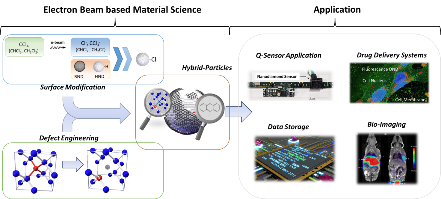
The sensors we develop subsequently should find explorative applications in:
- Data, automotive, and electronics industries, for example, as sensors for lithium batteries or as long-term data storage
- Biotechnology and medicine as drug delivery systems or as sensors for early tumor detection
- Heterogeneous catalysis, for example, as highly sensitive hydrogen sensors
Expertise
- Synthesis and modification of optically active nanoparticles and quantum sensors
- Radiation chemistry on surfaces and defects: defect engineering in solids
- Analysis and optimization of optical properties of nanoparticles
- Nanoparticle-polymer interfaces
- Design of selective optical sensor devices
Highlights
- Isotropic Scalar Quantum Sensing of Magnetic Fields for Industrial Application
R. Staacke; R. John; R. Wunderlich; L. Horsthemke; W. Knolle; C. Laube; P. Glösekötter; B. Burchard; B. Abel; J. Meijer, Adv. Quantum Technol. 2020, 3 (8), 2000037; DOI: https://doi.org/10.1002/qute.202000037
- Facet-selective etching trajectories of individual semiconductor nanocrystals
C. Yan, D. Byrne, J. C. Ondry, A. Kahnt, I. A. Moreno-Hernandez, G. A. Kamat, Z.-J. Liu, C. Laube, M. F. Crook, Y. Zhang, P. Ercius, P.A. Alivisatos, Science Advanced, 2022, 8, eabq1700. Fluorescence Lifetime Control of Nitrogen Vacancy Centers in Nanodiamonds for Long-Term Information Storage
C. Laube, R. Temme, A. Prager, J. Griebel, W. Knolle, and B. Abel, ACS Nano, 2023, 17 (16), 15401-15410.Radiation Chemistry-Based Molecule Grafting: A Fast Track to Diamond-Based Hybrid Sensors
C. Laube, I. Zwanck, M. Hanisch, L. Langguth, R. Staacke, R. Konieczny, A. Prager, J. Griebel, S. Zahn, W. Knolle, Chemistry of Materials, 2024, 36, 9, 4368-4378.13C hyperpolarization with nitrogen-vacancy centers in micro- and nanodiamonds for sensitive magnetic resonance applications
R. Blinder, Y. Mindarava, M. Korzeczek, A. Marshall, F. Glöckler, S. Nothelfer, A. Kienle, C. Laube, W. Knolle, F. Jelezko, Science Advanced,2025,11, eadq6836.