Quantum technologies are currently a hot topic in fundamental and applied research. The exploitation of quantum mechanical phenomena for information processing or highly accurate sensors enables fundamentally new applications, for example in future secure communication. Promising quantum systems for sensor applications and quantum computing are single impurity atoms in solid state materials or a complex of an impurity atom with a defect, e.g. the NV-center in diamond. The fabrication of such quantum objects requires new and innovative technologies, for example based on ion implantation. The aim of the work, therefore, is the development of an ion implanter for placing single counted ions (deterministic ion implantation) with a lateral precision at the nanoscale. Both is a prerequisite for the functionalization of the impurity atom in a quantum device and the fabrication of quantum devices that are based on regular arrangements of many of these quantum objects.
The work is done within the Leibniz Joint Lab “Single ion implantation” together with the work group “Applied Quantum Systems” of Prof. Jan Meijer at Leipzig University.
Expertise
- Development and optimization of image charge detection of ion bunches and single highly charged ions
- Optimization of ion optics for focusing highly charged ions from an electron beam ion source
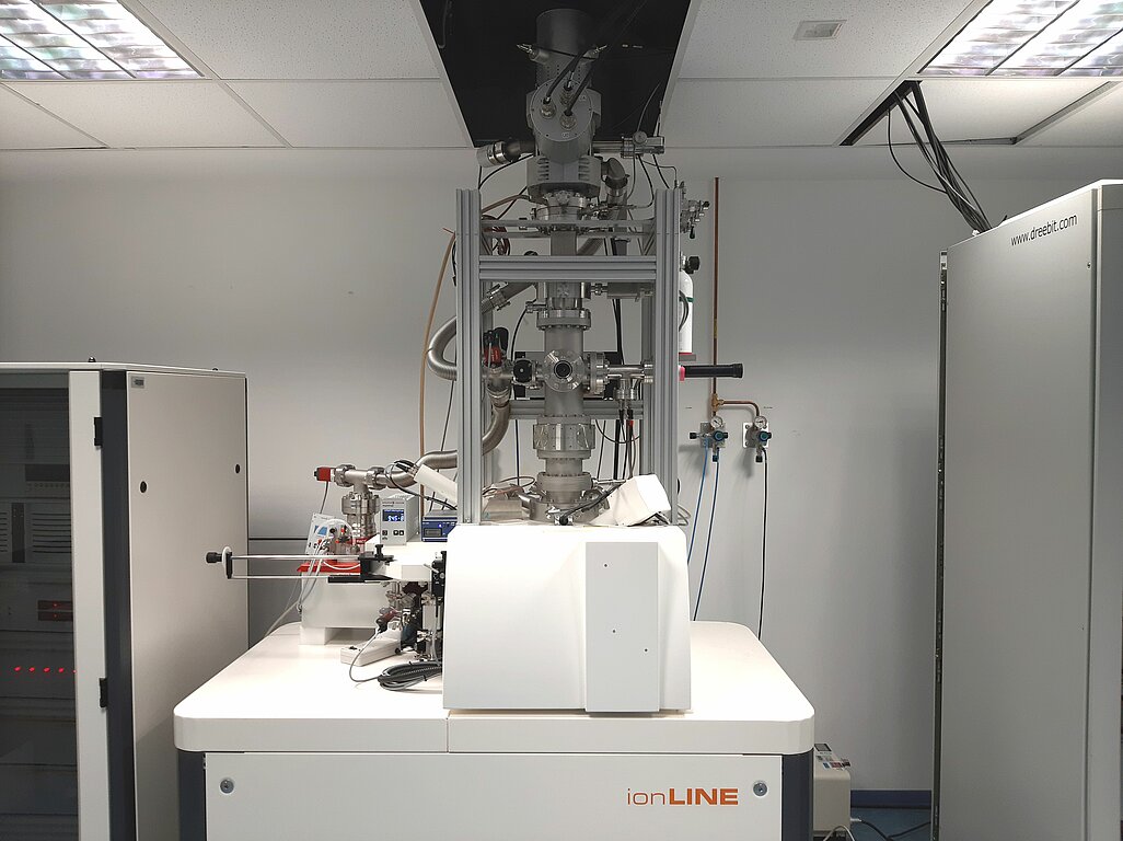
- Mask-free implantation of ions for a wide range of kinetic energies and charge states
- Local defect production in solid state materials via mask-free ion irradiation
Highlights
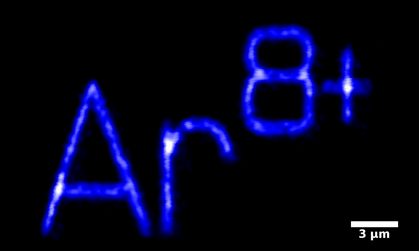
Nanoscale ion implantation using focussed highly charged ions
P. Räcke, R. Wunderlich, J.W. Gerlach, J. Meijer, D. Spemann
New Journal of Physics 22 (2020) 083028
DOI: 10.1088/1367-2630/aba0e6Ion implantation is not only an established technique for semiconductor industry and research, but also a key method enabling ground-breaking research in novel quantum technologies like quantum sensing and computing, e.g. based on donors in silicon or the nitrogen-vacancy-(NV)-centre in diamond. For the realisation of quantum computing, a main challenge is the scalability of the qubit fabrication. For ion implantation, this means combining a high throughput with spatially precise placement of a counted number of single dopants or defects is crucial. For this purpose, a focussed ion beam (FIB) based ion implanter equipped with an electron beam ion source (EBIS) able to produce highly charged ions was set up. The ion optical system was optimised and beam spot sizes below 200 nm achieved, showing that nanoscale ion implantation using an EBIS is feasible. As an example of its utilisation, we demonstrate the direct writing of nitrogen-vacancy centres in diamond using mask-less irradiation with focussed Ar8+ ions with sub-micron three-dimensional placement accuracy.
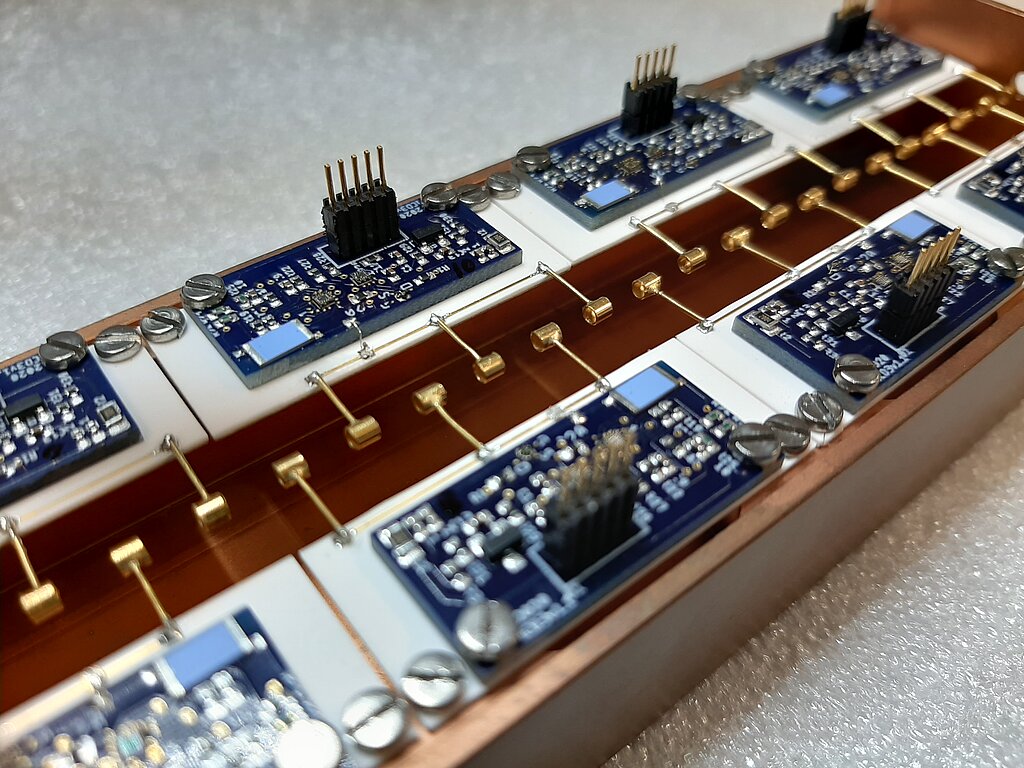
Image charge detection statistics relevant for deterministic ion implantation
P. Räcke, R. Staacke, J.W. Gerlach, J. Meijer, D. Spemann
J. Phys. D: Appl. Phys. 52 (2019) 305103 (5pp)
DOI: 10.1088/1361-6463/ab1d04Image charge detection (ICD) is a technique that can be used to non-perturbatively measure the velocity, charge, mass and other properties of moving charged particles. Image charge detection can also be used as a non-perturbative pre-detection approach for deterministic ion implantation. Using low energy ion bunches as a model system for highly charged single ions, we experimentally studied the error and detection rates of an image charge detector setup. The probability density functions of the signal amplitudes in the Fourier spectrum can be modelled with a generalised gamma distribution to predict error and detection rates. It is shown that the false positive error rate can be minimised at the cost of detection rate, but this does not impair the fidelity of a deterministic implantation process - this is a specific advantage of the pre-detection approach where the ion detection is independent from the implantation itself. Independent of the ion species, at a signal-to-noise ratio of 2, a false positive error rate of 0.1% is achieved, while the detection rate is about 22%. A detection rate of 22% means that 22% of all ions moving through the detector are detected and passed on to the implant site whereas the remaining 78% of the ions are automatically discarded by a beam blanker.
Detection of small bunches of ions using image charges
P. Räcke, D. Spemann, J.W. Gerlach, B. Rauschenbach, J. Meijer
Scientific Reports 8 (2018) 9781
DOI: 10.1038/s41598-018-28167-6Deterministic ion implantation enables the placement of single counted impurity atoms into a host material where they can be functionalized and used as quantum objects, for example, in quantum sensing or quantum computing. The ability to control the exact number of atoms implanted into a specific location is a prerequisite for the fabrication of quantum devices that rely on a set of individual quantum objects like qubits. The detection of each implanted ion can be done before the implantation itself (pre-detection) or during the implantation process (post-detection) exploiting secondary effects from the ion stopping in the host material. The latter approach, therefore, depends on the specific properties of the host material, whereas a pre-detection approach does not.
Here, a concept for detection of charged particles in a single fly-by, e.g. within an ion optical system for deterministic implantation, is presented. It is based on recording the image charge signal of ions moving through a detector, comprising a set of cylindrical electrodes. This work describes theoretical and practical aspects of image charge detection (ICD) and detector design and its application in the context of real time ion detection. It is shown how false positive detections are excluded reliably, although the signal-to-noise ratio is far too low for time-domain analysis. This is achieved by applying a signal threshold detection scheme in the frequency domain, which - complemented by the development of specialised low-noise preamplifier electronics - will be the key to developing single ion image charge detection for deterministic implantation.Apparatus for detecting individual charged particles and material processing system having such an apparatus
Jürgen W. Gerlach, Jan Meijer, Sébastian Pezzagna, Bernd Rauschenbach, Stephan Rauschenbach, Daniel Spemann, (2018) (EP16723276.8), EPA
Patent specificationThis patent details a setup for the detection of a single, charged particle, e.g. an ion, in a single pass through a set of electrodes such that the trajectory of the particle is practically undisturbed. The latter is a prerequisite for an ion optical image formation that allows for a lateral placement accuracy of the ion at the nanoscale. The detection approach relies on a regular arrangement of electrodes in which the passing ion influences an image charge. This image charge can be amplified and results in an alternating signal of specific frequency that can be measured. This approach is the foundation for the single ion detection required for the deterministic ion implantation developed at the Institute.
Near-Surface Electrical Characterization of Silicon Electronic Devices Using Focused keV-Range Ions
S.G. Robson, P. Räcke, A.M. Jakob, N. Collins, H.R. Firgau, V. Schmitt, V. Mourik, A. Morello, E. Mayes, D. Spemann, and D.N. Jamieson
Physical Review Applied 18, 034037 (2022)
DOI: 10.1103/PhysRevApplied.18.034037When phosphorus or other donors are introduced into high-purity silicon by means of single ion implantation, they form a promising quantum bit (qubit) system for the development of a scalable quantum computer. However, what is needed for scalability is a method for deterministic ion implantation. For this purpose, our collaboration partners from the CQC2T of the School of Physics, University of Melbourne are developing dedicated silicon substrates to detect each individual ion during implantation using IBIC (Ion Beam Induced Charge).
This paper reports on the results of a collaborative work of CQC2T members and colleagues from IOM. Here, the feasibility of single ion detection via IBIC is explored by implanting low-energy ions into silicon devices featuring a 60 × 60 μm2 sensitive area and an ultrathin 3.2-nm gate oxide—capable of hosting large-scale donor arrays. An IBIC-mapping system consisting of a modified focused-ion-beam machine and ultralow-noise ion-detection electronics is employed to demonstrate the capability for evaluating the device response characteristics to shallowly implanted 12-keV 1 H2+ ions. Despite the weak internal electric field, near-unity charge collection efficiency is obtained from the entire sensitive area. The approach is then adapted to perform deterministic implantation of a few thousand 24-keV 40Ar2+ ions into a predefined microvolume, without any additional collimation. Despite the reduced ionization from the heavier ion species, a fluence-independent detection confidence of ≥99.99% is obtained. Our system thus represents not only a method for mapping the near-surface electrical landscape of electronic devices but also a framework toward mask-free prototyping of large-scale donor arrays in silicon.
Projects and networks
Development and realisation of a single ion detector for deterministic ion implantation
The goal of the project was investigating the potential and technical realization of an image charge detector for detecting single ions with only a single pass through the detector. Such a detector enables deterministic ion implantation, i.e. the highly precise placement of single counted ions in surface-near regions of practically any substrate for applications in quantum technologies. For this purpose, suitable ultra-low noise electronics based on silicon and GaAs transistors was investigated and optimized regarding noise performance and sensitivity in a test setup. In parallel, the beam transport in the ionLINE implanter was configured for integration of the image charge detector. After its optimization and integration in the ionLINE the image charge detector shall be characterized under cryogenic operation regarding detection sensitivity. Finally, the data shall be used to critically evaluate the potential of image charge detection for single ion detection and a detailed technical realization of such a detector shall be proposed.
The work is done in collaboration with the Universität Leipzig in the Leibniz Joint Lab "Single ion implantation".
Duration: 2017-2020
Funding: 314.477,00 Euro
Funding programme: Sächsische Aufbaubank (SAB)
Cooperation Partner: Universität LeipzigSee also under "Selected projects"
EU Cost Action FIT4NANO
The aim of the Action “Focused Ion Technology for Nanomaterials” (FIT4NANO), is to create a coordinated effort in the field of ion beam based nanoengineering that will put European researchers and commercial businesses at the forefront of the quickly moving field of functional nanostructured materials.
The Action will unite developers and practitioners of focused ion beam technology to enable them to build the most efficient tool sets and application techniques for the identification, fabrication and characterization of next generation functional nanomaterials, as well as develop ion sources and instrumentation for the sub 10 nm fabrication and materials analysis.More information can be found under https://www.fit4nano.eu/