Micro and nano structures are become increasingly important for technical applications and in everyday’s life, e.g. for clean surfaces, illumination technology, safety and in reducing friction and wear. Research at the IOM focuses on the production of precise surfaces, preferably by material ablation or etching (glass, plastics and metals) with pulsed laser radiation. The high accuracy needed for applications in the field of optics requires the development of methods and processes that enable precise depth adjustment, minimal roughness, and low material damage. This involves developments at the intersection of physical and chemical processes that are laser-guided and thus enable the computer-accurate writing of patterns, structures and shapes with sizes ranging from 1 µm to 20 cm, thus bridging the gap to industrial applications.
Expertise
- Direct structuring, texturing and modification of surfaces with short and ultra-short pulse lasers
- Development and optimisation of laser processes for precise structuring, shaping and figuring of surfaces in glasses and plastics with low surface damage and low roughness
- Development of beam shaping and machining methods for precise laser material processing
- Process development of laser material etching methods in reactive gases and liquids
- Laser structuring of masters for copying processes
Highlights
Laser-induced backside wet etching of transparent materials with organic and metallic absorbers
K. Zimmer, R. Böhme
Laser Chemistry (2008) 170632
https://doi.org/10.1155/2008/170632Laser-induced backside wet etching (LIBWE) allows the high-quality etching of transparent materials for micro- and nanopatterning. Results on LIBWE with hydrocarbon and metallic absorbers are summarized discussing the impact of the liquid absorber, the material, the wavelength, and the pulse length of the laser to the material etching. In particular, the etching of submicron-sized periodic structures in sapphire and fused silica with interference techniques and the selection of the preferred etching method in dependence on the material and the processing goal is reviewed. The experimental results are discussed with a thermal model considering surface modification and near-surface laser ablation in confinement to a liquid.
Laser-induced reactive microplasma for etching of fused silica
M. Ehrhardt, P. Lorenz, B. Han, K. Zimmer
Applied Physics A - Materials Science & Processing 126 (11) (2020) 9
https://doi.org/10.1007/s00339-020-04019-xHigh-quality, ultra-precise processing of surfaces is of high importance for high-tech industry and requires a good depth control of processing, a low roughness of the machined surface and as little as possible surface and subsurface damage. These demands usually cannot realized by laser ablation processes. Hence, a combined approach of laser and plasma processing is proposed and demonstrated that enable the machining of surfaces with high quality. The focusing of laser radiation into a reactive gas, which can also be air, optical breakdown occurs and a laser-induced reactive microplasma is generated that is used here to etching of fused silica at normal pressure.
Hence, the process combines advantages of laser processing and plasma technology. Therefore, the experimental results contribute to the development of new fabrication technologies that enable emerging machining processes for optical or microtechnical applications.Studies on perovskite film ablation and scribing with ns-, ps- and fs-laser pulses
L. Bayer, X. Ye, P. Lorenz, K. Zimmer
Applied Physics A 123 (10) (2017) 619
https://doi.org/10.1007/s00339-017-1234-5Hybrid organic–inorganic perovskites attract much attention due to their exceptional optoelectronic properties, in particular for photovoltaic (PV) applications. The accurate, high-speed and reliable patterning of the PV films is required for perovskite solar modules fabrication. Laser scribing provides these characteristics needed for industrial fabrication processes. In this work, the laser ablation and scribing of perovskite layers with different laser sources (ns-, ps-, fs-laser pulses with wavelengths of 248 nm to 2.5 µm) were systematically investigated. The patterning results of the perovskite film can be classified into (1) regular laser ablation, (2) thin-film delamination lift-off process, and (3) lift-off with thermal modifications. A particular process, the localised lift-off of single grains from the perovskite film, has been observed and is discussed in relation to the thin-film lift-off process. Laser scribing of the perovskite layer is favorable for module interconnection via P2.
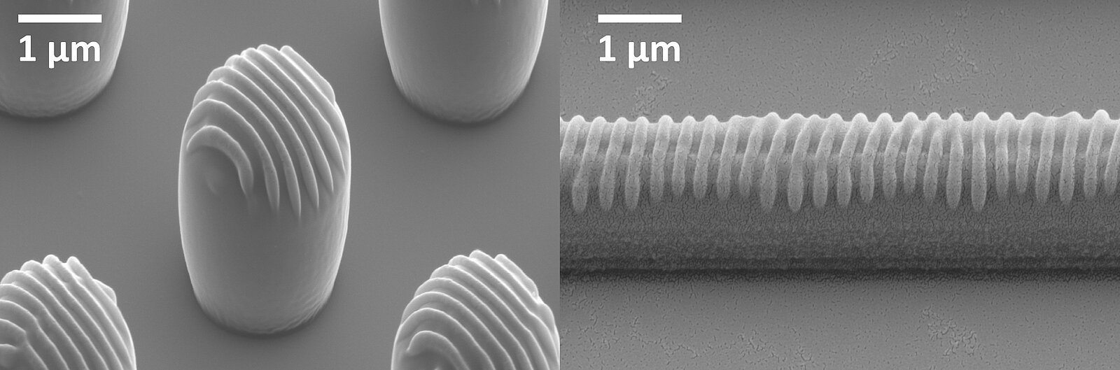
Towards fast nanopattern fabrication by local laser annealing of block copolymer (BCP) films
K. Zimmer, J. Zajadacz, F. Frost, A. Mayer, C. Steinberg, H. F. Chang, J. Y. Cheng, H. C. Scheer
Applied Surface Science 470 (2019) 639-644
https://doi.org/10.1016/j.apsusc.2018.11.105Self-assembly and self-organisation processes enable mechanisms for direct pattern generation in materials and thus offer good conditions for large-area and cost-effective structure generation. Since nanopatterning of surfaces below 100 nm is challenging, laser-assisted self-assembly of polymeric surfaces with structure dimensions of 25 nm is demonstrated here.
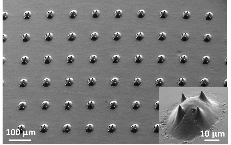
Laser annealing of PS-b-PMMA block copolymer films results in laser-guided local self-assembly at irradiation times below 0.1 s. In the paper, the observed processes and mechanisms of self-assembly in such films are demonstrated and discussed. The short-time assembly process in the diblock copolymer layer triggered by the laser-induced temperature field enables the direct writing of hierarchical nano/microscale structures required for bio-inspired applications.Laser patterning of hierarchical structures on metal cylinders for UV-NIL replication
P. Lorenz, L. Bayer, T. Tachtsidis, K. Zimmer
Bayerisches Laserzentrum GmbH, 10th CIRP Conference on Photonic Technologies [LANE 2018] 1-4
https://www.lane-conference.org/industrial-contributions-2018Functional, micropatterned surfaces are required in diverse fields of applications such as self-cleaning, illumination and biocide surfaces. Such applications require the cost-effective fabrication of structures into functional materials with a high throughput. Ultraviolet nanoimprint lithography (UV-NIL), which can be integrated in a roll-to-roll (R2R) process, opens the way for the industrial fabrication of such functional micro- and nanostructures in large scale. Laser processing, however, allows the computer-controlled individual patter writing onto master cylinders needed for the R2R process.
Here we report on laser writing of hierarchical patterns, seamless on nickel sleeves (360°) using ps - laser with wavelengths of 1064 nm and 355 nm. A lateral overlay accuracy of the 30 µm and 6 µm hole arrays forming periodic hierarchical patterns of better than 10 µm was determined over large areas at the cylinder.