Gallium oxide (Ga2O3) is a promising semiconductor material for use in high-power electronics, UV detectors, and gas sensors. It is a fourth-generation semiconductor oxide, which has an extremely large band gap and a high electric breakdown voltage. Therefore, it has been the focus of intensive investigations since some years.
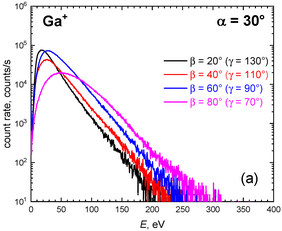
Researches at IOM want to contribute to these activities by investigationg the opportunities of ion beam sputter deposition for the growth of high-quality Ga2O3 thin films. In a first study, IOM researchers have investigated the properties of particles, which are produced during ion beam sputtering of a Ga2O3 target, in dependence on various process parameters, such as sputtering geometry, incident ion species and energy, process gas pressure. These particles bring energy to the growing film during deposition, and knowledge of their energies is of great benefit for understanding the process and tailoring thin film properties.
The results have been published, recently, in Journal of Vacuum Science & Technology A:
Further information of the article:
Properties of secondary ions in ion beam sputtering of Ga2O3
Dmitry Kalanov, André Anders, Carsten Bundesmann
J. Vac. Sci. Technol. A, 2021, 39, 053409
https://avs.scitation.org/doi/10.1116/6.0001204
The preprint is also available:
https://www.researchgate.net/publication/353994196

