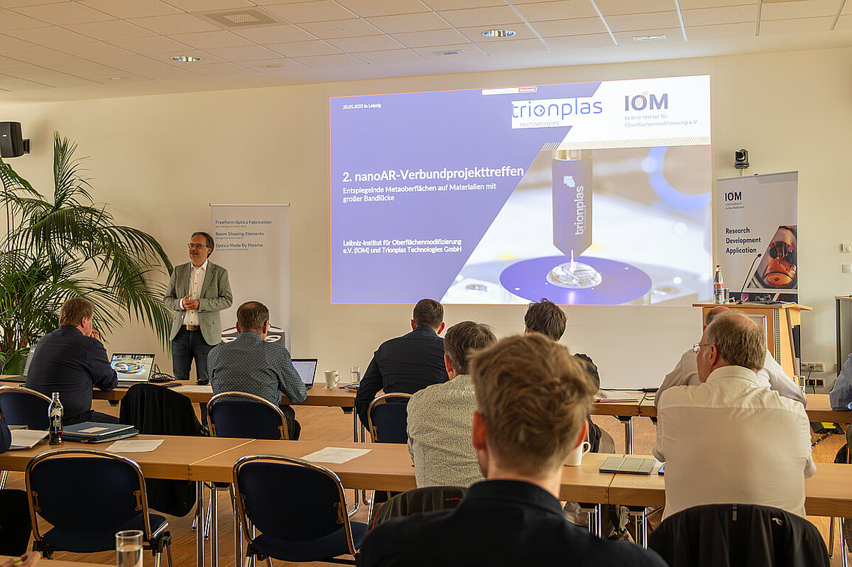
On May 20, 2025, the partners of the pioneering “nanoAR” research project met in Leipzig for their second joint meeting. The event was hosted by the Leibniz Institute of Surface Engineering (IOM) and Trionplas Technologies GmbH.
The event was opened by Prof. Dr. Benjamin Dietzek-Ivanšić, Scientific Director of the IOM, and Hendrik Paetzelt, Managing Director of Trionplas. The focus was on intensive technical exchange between the project partners from science and industry – driven by a shared vision: to help shape the future of energy.
After an overview of the current status and objectives of the project by the project coordinator, subsequent presentations and discussions reflected on the work done so far, shared insights, and coordinated next steps. It became clear that “nanoAR” thrives on close interdisciplinary cooperation between all participants. This was followed by an exciting tour of the host's facilities, during which participants explored the ion source laboratory, the RIBE450 ion beam etching system, the universal diagnostic platform for reactive ion beam processes, and a roll-to-roll coating system in the IOM's application center. The plasma jet systems from Trionplas Technologies GmbH were also presented. The direct view into the laboratories provided practical insight into the technological developments of the project partners and inspired new approaches for joint project work.
The “nanoAR” project brings together nine partners from industry and science with a common goal: to develop high-performance optical components for use in laser fusion power plants. In doing so, the participants are making a key contribution to the energy supply of the future.
With funding of six million euros from the German Federal Ministry of Research, Technology, and Space (BMFTR), “nanoAR” is a key project on the road to realizing optical components for use in laser fusion power plants. By 2027, expertise along the entire innovation chain will be pooled: from damage reduction in optical materials and precision structuring at the nanometer level to quality assurance using state-of-the-art diagnostics.
The second joint meeting was a day full of insights, ideas, and inspiration, and another important step in the joint research and development process of this ambitious project.
Link for further information.