![[Translate to English:]](/fileadmin/_processed_/b/8/csm_2026_Foerderhinweis_v2_8cd0f05c8b.png "[Translate to English:]")
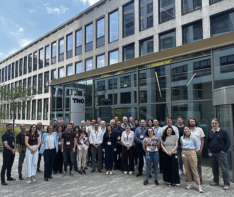
How can semiconductor technologies be advanced beyond today’s limits of miniaturization? This is the question addressed by the European research project “10 Ångstrom CMOS Exploration” (10ÅCe), whose consortium met on 27 and 28 May 2026 at project partner TNO in Delft.
After 24 months of project work, the meeting focused on current results from the work packages, technological challenges, and the next steps. The project is funded under Horizon Europe and is part of the Chips Joint Undertaking (Chips JU). Building on the predecessor project IT2 – Information and Communication Technology for the 2 nm Node, 10ÅCe develops approaches for future 10 Å CMOS chip technologies. The consortium brings together leading European partners from research and industry and covers key areas of the value chain — from chip design and lithography to process technology and metrology.
Dr. Frank Frost, head of the IOM working group “Ion Beam Assisted Patterning and Smoothing”, and Peter Birtel, research associate, attended the meeting on behalf of the institute. They presented current results on the further development of the EUV tool, particularly with regard to enabling smaller pitches and improving yield. With its long-standing expertise in ion beam assisted etching, patterning, and smoothing, IOM contributes to ultra-precise manufacturing approaches for next-generation optical and semiconductor-related applications.
The meeting in Delft underlined the importance of European cooperation for the future of microelectronics. Through consortium meetings such as this one, 10ÅCe strengthens the close connection between fundamental research, technological development, and industrial application. The project demonstrates that the next generation of semiconductor technologies can only be achieved through coordinated European efforts, the exchange of expertise, and long-term strategic cooperation. For IOM, participation in this consortium means contributing to a field that is of crucial importance for Europe’s technological sovereignty and future competitiveness.
A particular highlight was the tour of TNO’s research infrastructure. IOM warmly thanks Henk Lensen, Senior Project Manager at TNO for Semicon Equipment Lifetime and Metrology, for the excellent organization of the meeting and the impressive insights provided during the laboratory tour.