Ion beam assisted etching technologies are essential to realize ultra-precision structured as well as ultra-smooth surfaces on technologically relevant materials (optical glasses and glass ceramics, oxides, semiconductors, metals, polymers, layer systems). These processes are rapidly gaining importance in optics development and manufacturing, with precision requirements (shape, depth accuracy, roughness) now sometimes well below one nanometer. Taking these developments into account, the focus is on investigating the fundamentals of reactive and inert ion beam etching processes. In parallel, a technological implementation of the results and their transfer into application-ready processes and products for research institutions and industrial partners is pursued. For this purpose, it is necessary to further develop tools developed at the IOM, such as broad-beam ion sources and process simulation methods, and to adapt them to new requirements.
Expertise
- Fundamentals and application of (reactive) ion beam etching processes for the generation of nano- and microstructures
- Mechanisms and exploration of ion beam induced self-organization processes
- Ion beam assisted smoothing and planarization of surfaces
- Transfer of research results and technology steps
Highlights
Large area smoothing of surfaces by ion bombardment: fundamentals and applications
F. Frost, R. Fechner, B. Ziberi, J. Völlner, D. Flamm, A. Schindler
J. Phys. Condens. Matter 21 (2009) 224026
https://doi.org/10.1088/0953-8984/21/22/224026
Ion beam erosion can be used as a process for achieving surface smoothing at microscopic length scales and for the preparation of ultrasmooth surfaces, as an alternative to nanostructuring of various surfaces via self-organization. This requires that in the evolution of the surface topography different relaxation mechanisms dominate over the roughening,and smoothing of initially rough surfaces can occur. This contribution focuses on the basic mechanisms as well as potential applications of surface smoothing using low energy ion beams.Ion beam planarization of diamond turned surfaces with various roughness profiles
Y. Li, H. Takino, F. Frost
Opt. Express 25 (2017) 7828-7838
https://doi.org/10.1364/OE.25.007828The effectiveness of ion beam planarization (IBP) to reduce surface roughness of diamond turned NiP surfaces was investigated. It is found that the combined process of spray-coating and ion-beam planarization can effectively reduce the surface roughness of diamond turned NiP. The final surface roughness after ion beam planarization is 30%~40% of the original roughness, irrespective of spatial wavelength and depth of turning marks. Extending planarization time does not alter surface quality after photoresist is etched away. These results show that the IBP is applicable to roughness minimization of diamond turned surfaces.
Realization of depth reference samples with surfaces amplitudes between 0.1 nm and 5 nm
A. Finzel, G. Dornberg, S. Görsch, M. Mitzschke, J. Bauer, F. Frost
EPJ Web. Conf. EOS Optical Technologies 215 (2019) 03004
https://doi.org/10.1051/epjconf/201921503004A new approach for the realization of depth reference samples is presented. By a combination of photolithography, reactive ion beam etching, surface planarization with photoresists and a subsequent coating with non-transparent materials, defined sinusoidal surface profiles are generated which can be used as depth references for the comparison and calibration of different surface profile measurements. The smallest realized surface amplitudes are in the range of less than 0.1 nm.
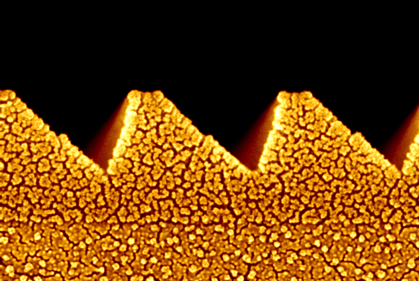
Terrace morphology on fused silica surfaces by Ar+ ion bombardment with Mo co-deposition
D. Chen, G. Yang, J. Li, D. Hirsch, Y. Liu, F. Frost, Y. Hong
Appl. Phys. Lett. 113 (2018 ) 033102
https://doi.org/10.1063/1.5039565
The morphology evolution of self-organized nanopatterns induced during Ar+ ion bombardment (IB) with Mo co-deposition on fused silica (SiO2) surfaces at different incidence angles and fluences was investigated by using atomic force microscopy and transmission electron microscopy. For pure IB at incidence angles from 30° to 70°, SiO2 surfaces evolve from being flat, via ripples, to direction-transversed ripples. In contrast, at the same ion fluence and incidence angles, the simultaneous Mo co-deposition leads to significant terraced structures with significantly enhanced roughness and wavelength. Our observations show that the concurrent Mo co-deposition during IB can reduce the critical incidence angle and the fluence level of terrace formation. Owing to the guidance of the IB-induced morphology, at incidence angles where a well-ordered ripple-mode can be generated, well-ordered terrace morphology is more likely to be formed.Reactive ion beam etching of highly dispersive, high-efficiency transmission gratings for the VIS range
A. Finzel, F. Koch, G. Dornberg, D. Lehr, F. Frost, T. Glaser
Opt. Eng. 58 (2019) 092614
https://doi.org/10.1117/1.OE.58.9.092614Reflection losses due to refractive index mismatch limit the obtainable diffraction efficiencies for transmission gratings in the highly dispersive regime, i.e., with period to wavelength ratios smaller than 0.7. The design and fabrication of such gratings with high-diffraction efficiencies (≥94%, Littrow configuration) will be discussed with an emphasis on process strategies to control the profiles in the reactive ion beam etching step. Experimental results from the manufacturing of monolithic fused silica pulse compression gratings with 3000 L∕mm optimized for a center wavelength of 519 nm will be presented. The influence of different etching parameters such as etch gas mixture, ion incidence angle, and acceleration voltage of the ion source on profile depth, side-wall angle, duty cycle, and ultimately diffraction efficiencies will be discussed.
Projects
Antireflective meta-surfaces on wide bandgap materials - nanoAR
2024-2027
In the “nanoAR” project, the project partners are combining their expertise in manufacturing and processing methods to effectively reduce SSD (subsurface damage) by means of technology-open process development for nanostructure generation, including the use of simulation and modeling, high-resolution material characterization and the development of new methods for quality assurance.Press release Link
Further information about the project LinkEU-Project "10ÅCe - 10 Ångstrom CMOS exploration"
Duration: 2024 – 2027
The objective of the EU project is to explore and realize solutions for the 10Å CMOS chip technology. The project consortium covers the entire value chain for manufacturing of the CMOS chips in the 10A node, that is, from chip design to lithography to process technology and finally chip metrology. Essential parts of hardware, software and processing technology are developed pushing the boundaries of semiconductor design and manufacture to enable the new node and keep Moore’s law alive.
Link: https://cordis.europa.eu/project/id/101139972BMBF "Monolithic binary and blaze lattices on silicon and oxides" (MOBBS)
Duration: 01/24 - 12/25
In a joint project funded by the BMBF and the GRAVOmer network, researchers from the IOM research area "Reactive Ion Beam Assisted Structuring and Smoothing", together with Carl ZEISS Jena GmbH and scia Systems GmbH, want to establish novel ion beam-based manufacturing processes with which inclined surface profiles (blaze profiles) for diffractive optical elements (DOE) can be realised that are not accessible with previous technologies. To this end, a new ion beam etching technology for the production of monolithic, blazed silicon diffraction gratings for beamline applications in the VUV, EUV and X-ray range is to be developed on the basis of lithographic structure definition. In particular, if successful, enormous performance increases can be realised through more sharply defined blaze edges, especially against the background of constantly decreasing blaze angles.
Press release Link
Further information about the project LinkNSF-DFG-Project AD-ION "Advances in ion-surface interaction-driven manufacturing of one-dimensional metal oxide heterostructures"


This project is dedicated to the exploration of methods for the advanced manufacturing of spatially coherent, homogeneous, and high-quality compound one-dimensional nano-heterostructures by principles of oblique angle deposition in combination with assist ion bombardment (iGLAD). One assist ion source implemented into the fabrication process will be subsequentially operated for i) substrate pre-patterning via ion erosion, ii) control of phase and stoichiometry via reactive ion bombardment, and iii) nanostructure size control via ion figuring. A hypothesis-driven approach is employed to investigate nucleation, growth, interface formation, surface patterning and nanostructure crafting for the fabrication of metal oxide nano-heterostructures in correlation to process parameters such as ion energy, ion current density, angle of incidence and ion mass, using ZrO2-MoO3-x as a model substance.
This proposal is based on mutual scientific interest in low-energy reactive ion beam processing for advanced additive manufacturing and combines expertise from Dr. Eva Schubert, Associate Professor at the University of Nebraska-Lincoln (U.S.A.) and Dr. Frank Frost, Head of Division for Ion Beam Assisted Patterning and Smoothing at the Leibniz Institute of Surface Engineering (IOM) in Leipzig (Germany). High resolution STEM imaging in combination with EDX elemental analysis will be conducted by Dr. René Feder, Team Manager Hybrid Systems, from IOM sub-contractor Fraunhofer-Institute for Microstructures of Materials and Systems in Halle/Saale.
EU-Projekt „IT 2 - IC Technology for the 2 nm Node”
In diesem industriegeführten ECEL-Projekt bringen insgesamt 32 Partner ihre Kompetenzen ein. Gesamtziel des IT2-Projekts ist die Erforschung, Entwicklung und Demonstration von Technologieoptionen zur Realisierung der 2 nm-CMOS-Logik-Technologie. Die Aktivitäten umfassen Lithographie, Prozess- und Modulexploration und Messtechnik. Das IOM entwickelt mit seinen Partnern einen optimierten Ionenstrahlprozess, einschließlich der notwendigen Werkzeuge für die hochpräzise Herstellung von strukturierten EUV-Optiken mit deutlich höherer Effizienz und zusätzlicher Unterdrückung unerwünschter Wellenlängenbereiche.
Link